Abstract
Nanoelectronics linear scaling appeals to new 3D integration schemes in order to continue Moore’s law. Unique opportunities exist to increase the device's performance, system complexity and also to reduce power consumption of mobile handheld objects. New design and functional architecture will be possible by mixing logic and memory devices to save power consumption and introduce new applications by using neuromorphic or bio inspired approaches. Devices other than CMOS can be co-integrated with CMOS to interface the outside Multiphysics world (MEMS, sensors and actuators, RF devices, power devices,etc.) allowing new functionalities. 3D Wafer Level Packaging and System on a Wafer allow these new routes.
Biography
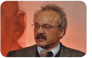
Simon Deleonibus received his MSc and PhD in Applied Physics from Paris University in 1979 and 1982, respectively. He joined LETI-CEA in 1986 as an expert in device engineering and process modules development for CMOS and Flash memories applications. Since joining LETI-CEA, he has managed the Ultimate CMOS project and was appointed Director of the Electronic Nanodevices Laboratory. Simon is currently the Chief Scientist (Directeur Scientifique) at CEA-LETI Silicon Technologies & Components. Simon has published over 550 papers and holds 32 patents, including the initial patent on contact plug principle. He has received numerous awards and honors, including being selected as an IEEE Fellow and IEEE Distinguished Lecturer and is the Research director at the French Alternative Energies and Atomic Energy Commission (CEA).