Quantum technologies are beginning to impact how society processes, stores, and transmits information, with recent demonstrations of a quantum computational advantage for specialized tasks, distributing entanglement between remote qubits, and satellite-based quantum communications. As quantum systems rapidly expand from a few quantum bits (qubits) to tens of thousands, integrated photonic and microelectronic technologies will play an important role in reducing the size, weight, power, and noise to enable scalable and energy efficient quantum technologies. Researchers in the Institute for Energy Efficiency are tackling the key challenges for achieving large scale quantum information technologies with low energy footprints for quantum computing, communications, networking, and sensing.
Grand Challenge
Outperform classical computers with >10,000X improvement in energy efficiency
An often overlooked, but equally important, advantage of quantum computing technologies is their energy footprint compared to classical machines. With their exponential improvement in computational power, quantum computers are already capable of performing specialized tasks in a fraction of the time required for a supercomputer with a fraction of the energy usage. As quantum systems begin to expand beyond the noisy intermediate-scale quantum (NISQ) era, increasing the complexity and scale while maintaining a low energy footprint will require reducing large, table-top experiments to chip-scale technologies.
IEE’s researchers are building photonic and microelectronic integrated hardware and full-stack software to solve some of the most difficult quantum engineering problems. These efforts include developing integrated photonic quantum computers using ultra-efficient photonic materials, heterogeneous integration of lasers and single-photon detectors with silicon photonics, interfacing atomic quantum systems onto photonic chips, and creating energy-efficient programming frameworks for emerging quantum computing technologies.
SUCCESS STORY
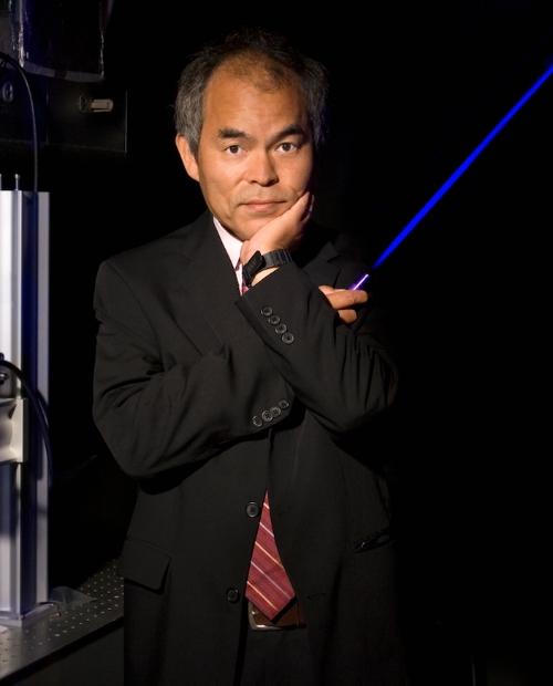
Dr. Shuji Nakamura Wins Nobel Prize for LED Breakthroughs
Shuji Nakamura and his team continue to expand the world of applications for his GaN based, high-efficiency, blue and green LEDs.
Focus Area
Technology and infrastructure enabling high-speed networks of quantum systems
Quantum information technologies are being developed across a wide-range of materials and systems, from superconducting circuits to atoms, defects in solids, and photonics. It is becoming increasingly clear that a hybrid approach that leverages the strengths of complementary quantum systems is necessary, which requires developing new technologies to interface them. This is challenging for several reasons, including their different operational regimes spanning microwave to optical frequencies and cryogenic to room temperature environments, as well as the requirement to maintain efficient communications, since loss of information destroys any potential quantum advantages.
Addressing these challenges is critical for overcoming the “interconnect bottleneck” facing quantum information technologies. Doing so requires a collaborative environment of scientists, engineers, and industry partners to connect quantum systems. IEE researchers are developing the frameworks and plug-and-play technologies for networking quantum systems leveraging the telecommunications fiber-optic infrastructure.
Focus Area
Ultralow Size, Weight, Power, and Cost (SWaP-C) systems for quantum communications
While we are likely at least a decade away from quantum computers capable of breaking RSA encryption, researchers and industry are actively developing algorithms and hardware for secure communications. Although quantum computing is still a nascent field, quantum communications is a near-term technology already commercially available. In particular, Quantum Key Distribution (QKD) hardware can enable more secure networks in which eavesdroppers would be detected or circumvented. Many existing quantum cybersecurity technologies are based on classical, benchtop technologies that require high-power lasers, amplifiers, and modulators, but future quantum communications systems will likely be deployable and both ground- and satellite-based.
IEE’s researchers are thus developing low SWaP-C integrated photonic technologies for secure communications. These include single-photon and entanglement-based quantum light sources, integrated lasers to pump the sources, and efficient on chip modulators and detectors for true plug-and-play, low footprint quantum transceivers.
Research Highlights
NSF Quantum Foundry (Professors John Bowers, Raphaële Clément, Galan Moody, Chris Palmstrøm, Ram Seshadri, and Chris Van de Walle) – Founded through the National Science Foundation’s Q-AMASE-i initiative, the Quantum Foundry at UC Santa Barbara is a next generation materials foundry that develops materials and interfaces hosting the coherent quantum states needed to power the coming age of quantum-based electronics. The mission of the Foundry is to develop materials hosting unprecedented quantum coherence, train the next generation quantum workforce, and to partner with industry to accelerate the development of quantum technologies.
UCSB Partnership with Cisco for Quantum Information (Professors Yufei Ding and Galan Moody) – A collaboration between UC Santa Barbara researchers and Cisco Systems aims to push the boundaries of quantum technologies. Assistant professors Yufei Ding and Galan Moody received research awards from the technology giant to work with its new Quantum Research Team, which was formed to pursue the research and development required to turn quantum hardware, software, and applications into broadly used technologies.
Quantum Workforce Development (Professors Yufei Ding and Galan Moody) – Among the many quantum education efforts on campus, two examples including the Quantum Photonics Learning Lab developed by Professor Moody to provide hands-on training in quantum information for undergraduates, graduates, and Santa Barbara City College students, as well as Professor Van de Walle’s Introduction to Quantum Materials course.
1,000-Fold Improvement in Entanglement Efficiency (Professors John Bowers and Galan Moody) – Professors Moody and Bowers demonstrated a 1,000-fold improvement in entangled-photon pair generation efficiency by replacing silicon chips with AlGaAs photonic chips. When scaling beyond a single source, these devices could reduce the energy footprint of quantum information technologies by many orders-of-magnitude.
Low-Loss Visible Photonics for AMO systems (Professor Daniel Blumenthal) – Professor Blumenthal’s group developed a low-loss, wafer-scale, CMOS-compatible photonic platform with wavelengths compatible with atoms, ions, and molecules commonly used for quantum information, sensing, and metrology applications.
